
Description
At-A-Glance Executive Brief
- Model: 810-105035-003
- Brand: Lam Research
- Part Type: PCB printed circuit board assembly (PCBA) for Lam semiconductor plasma etch equipment
- Lifecycle status: Legacy semiconductor fab spare; stocked for brownfield Lam etch tool maintenance & retrofits
- System compatibility: Lam Research wafer etch platform; handles chamber sensor signal conditioning, actuator control, serial bus communication between tool controller and process chamber, feeds telemetry/alarms to fab host
- Weight: ~0.32 kg
Technical Introduction
Failure of 810-105035-003 will disrupt chamber control and signal communication on the Lam etch tool. The board cannot read chamber pressure, gas or temperature sensors, or drive associated actuators. The tool triggers critical chamber fault alarms, recipe execution aborts, and wafer processing stops, resulting in fab production downtime and potential scrap wafers.
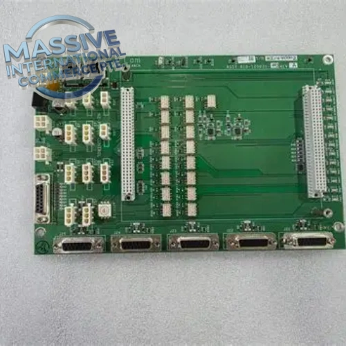
Lam Research 810-105035-003 is a custom plug-in PCBA designed for Lam plasma etch wafer processing systems. It acts as a chamber interface control board to acquire analog and binary sensor signals from the process chamber, perform signal conditioning, and communicate data over the tool backplane bus to the main system controller. The board outputs control signals to gas valves, solenoids and other chamber actuators, while collecting diagnostic health data and process telemetry. It supports real-time fault detection and sends alarm status to the tool HMI and fab host system. The PCB uses conformal coating to resist corrosive process vapors and humidity inside semiconductor equipment cabinets. Semiconductor fab maintenance teams stock 810-105035-003 to rapidly restore chamber control function during planned PM or unplanned board failures.
- Best Suited For
- Lam Research plasma etch wafer processing equipment
- Chamber sensor acquisition, actuator drive, backplane bus communication and process diagnostics
- Direct drop-in replacement for existing Lam Research 810-105035-003 PCB assembly hardware
Core Technical Specifications
| Parameter | Value |
|---|---|
| Part Number | 810-105035-003 |
| Manufacturer | Lam Research |
| Product Type | PCBA / Chamber Interface Control Board |
| Platform | Lam Plasma Etch Semiconductor Wafer Tool |
| Signal Types | Analog input, discrete I/O, serial backplane communication |
| PCB Treatment | Conformal coated |
| Power | Backplane DC supply |
| Operating Temp | 10℃ ~ 50℃ (cabinet ambient) |
| Humidity | 5–80% RH non-condensing |
| Feature | Built-in self-test, fault diagnostics, ESD protected circuitry |
| Mounting | Slot mount inside tool electronics cabinet |
| Weight | ~0.32 kg |
| Environmental Details | Please refer to the OEM datasheet for complete environmental tolerances. |
Field Engineer’s Tech Notes
- Confirm tool model, chamber revision, firmware version and board revision compatibility before replacement; mismatched revisions cause communication or recipe errors.
- Perform tool safe state, lockout/tagout and purge procedures before cabinet access; hazardous process gas and RF energy hazards exist.
- Inspect backplane connector pins for bending, corrosion or contamination; poor connector contact is a leading cause of intermittent signal faults.
- After installation, run board self-test, verify sensor readings and actuator control, execute chamber simulation, confirm HMI alarm reporting and clear faults before returning tool to wafer production.
- Strict ESD controls are mandatory during PCB handling; semiconductor PCBA components are extremely sensitive to electrostatic discharge.
- Inspect cabinet cooling filters regularly; dust buildup and overheating are common failure modes for coated Lam control boards.
Adaptive QA & Testing Protocol
Each 810-105035-003 PCBA is bench tested on Lam compatible test fixture. We verify DC power-up, backplane bus handshake, analog and discrete I/O response, actuator drive functionality and self-test diagnostics. Communication to tool controller is validated. PCB, edge connector and solder joints are visually inspected for corrosion, scratches, component burn marks or coating damage. Full test reports are available upon request.
Buyer’s FAQ
Q: What is Lam Research 810-105035-003 used for? A: It is a chamber interface PCB assembly for Lam plasma etch semiconductor tools, responsible for chamber sensor acquisition, actuator control and backplane communication with the main tool controller.
Q: What warranty applies for refurbished and NSFP 810-105035-003? A: Refurbished and NSFP units carry a 12-month hardware warranty. Coverage excludes ESD damage, process chemical corrosion, backplane surge damage, bent connector pins and revision mismatch configuration errors.
Q: What lead time should I expect? A: Stocked units ship 3–7 business days. If inventory is depleted, we source surplus Lam Research 810-105035-003 assemblies.
Q: Can I hot-swap this board while the tool is processing wafers? A: Hot swap is not supported. The tool must be placed in safe state and locked out before removing or installing this PCBA.

 Start Chat


 Send an Email


